India’s Tech Sovereignty Play: Decoding the ₹1.89 Lakh Crore Push for Semiconductor Phase 2 and Mobile Manufacturing
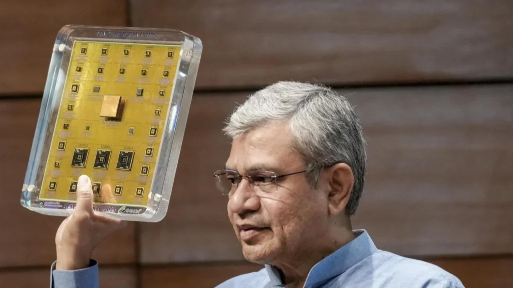
In a bid to cement its position as a global electronics and semiconductor hub, the Union Cabinet has greenlit the second phase of the India Semiconductor Mission (ISM 2.0) alongside a renewed Mobile Phone Manufacturing Scheme (MPMS). With a combined financial outlay of ₹1.895 lakh crore (approximately $22.7 billion)—broken down into ₹1.27 lakh crore for ISM 2.0 and ₹62,500 crore for MPMS—the twin initiatives represent a highly strategic, long-term bet by the Indian government.
The overarching objective is to build a self-sustaining domestic tech ecosystem. Over its five-year tenure, the government projects that these schemes will catalyze ₹4 lakh crore ($48 billion) in private investments, generate ₹2 lakh crore in domestic production, and drive ₹1 lakh crore in exports.
Chronology: The Evolution of India’s Electronics Policy
India’s journey toward high-tech self-reliance has moved from assembly-focused incentives to a deep-tech, ecosystem-wide strategy.
[Dec 2021: ISM Phase 1 Launched] ──> [2022: 50% Capital Subsidy Amendment] ──> [July 2025: ISM Phase 2 & MPMS Approved]
       (₹76,000 Crore Outlay)                (Attracted Micron, Tata Fab)              (₹1.89 Lakh Crore Combined Outlay)
Phase 1: Laying the Groundwork (December 2021–2024)
- December 2021: The Union Government approved the first phase of the India Semiconductor Mission with a fiscal commitment of ₹76,000 crore.
- Late 2022 Amendment: Recognizing intense global competition from the US, EU, and East Asia, the government modified the scheme to offer a uniform 50% capital subsidy on a "pari-passu" (equal footing) basis for silicon fabs, display fabs, and packaging units. This adjustment successfully attracted global giants, notably Micron Technology’s memory packaging plant in Sanand, Gujarat, and the Tata Group’s mega-fab in Dholera.
- Parallel Initiatives: The government also introduced the Electronics Component Manufacturing Scheme to incentivize the production of smaller passive components, resistors, and printed circuit boards (PCBs).
Phase 2: Expanding the Scope (July 2025 onward)
- July 15, 2025: The Union Cabinet approved ISM 2.0 and the MPMS, shifting focus from merely attracting assembly plants to building a comprehensive upstream and downstream supply chain.
- August 2025 (Expected): The official Gazette notification detailing the precise operational guidelines, eligibility criteria, and disbursement mechanisms for Phase 2 is slated for publication.
Supporting Data: Quantifying the Semiconductor Shift
To understand the scale of India’s ambitions, it is necessary to look at the concrete outcomes of Phase 1 and the targeted metrics of Phase 2.
Phase 1 Outcomes at a Glance
Under Phase 1, the government approved 12 manufacturing and packaging units, securing a total committed investment of ₹1.64 lakh crore.
| Project Type | Approved Units | Key Locations | Notable Projects |
|---|---|---|---|
| Semiconductor Packaging (ATMP/OSAT) | 9 | Gujarat, Uttar Pradesh, Punjab, Assam, Odisha, Andhra Pradesh | Micron (Gujarat), Tata-ASAT (Assam) |
| Silicon Fabrication (Fab) | 1 | Dholera, Gujarat | Tata Electronics (Commercial production by 2028) |
| Specialty Display Fab | 1 | India | Gallium-Nitride (GaN) Micro LED display fab |
| Design-Linked Incentive (DLI) | 24 | Nationwide (Startups/MSMEs) | Various domestic fabless chip design firms |
Technical Focus: Legacy vs. Frontier Nodes
A critical debate in India’s semiconductor policy centers on the complexity of the chips being manufactured.
- Frontier Nodes (<7 nanometers): Used in high-end smartphones, AI accelerators, and supercomputers. These require billions of dollars in highly specialized lithography equipment (such as ASML’s EUV machines) and extreme operational expertise.
- Legacy Nodes (28nm to 90nm and above): These chips power everyday electronics, automotive systems, IoT devices, medical hardware, and industrial equipment.
ISM Phase 1 and Phase 2 strategically target 28nm and older legacy nodes. The economic rationale is clear: the global market for legacy nodes is massive, highly resilient, and less capital-intensive to establish than frontier nodes. However, the roadmap for ISM 2.0 explicitly outlines a gradual transition toward smaller, more advanced nodes as the domestic ecosystem matures.
Official Responses and Policy Calibration
India’s policymaking apparatus has adapted its strategy based on the practical lessons learned during Phase 1.
Gradual Reduction in Subsidies
While Phase 1 offered a flat 50% capital subsidy, ISM 2.0 will trim this fiscal support to 30–40%.

Amitesh Kumar Sinha, Additional Secretary at the Ministry of Electronics and Information Technology (MeitY), explained the rationale behind this adjustment:
"The semiconductor industry is likely to get more attractive in India even with fewer incentives. As the baseline infrastructure, talent pipeline, and supplier networks mature, the perceived risk of investing in India decreases, allowing the state to optimize its fiscal resources."
Shift in Land and Infrastructure Support
In a positive development for cooperative federalism, the Union government is scaling back its direct involvement in land provisioning. State governments have begun actively competing to host semiconductor projects, offering land at token prices, subsidized water, uninterrupted power, and supplementary state-level capital subsidies.
Focus on Legacy Nodes and Ecosystem Breadth
Union Minister for Information Technology, Ashwini Vaishnaw, addressed critics who argue that India should skip legacy nodes and focus entirely on sub-7nm chips:
"There is a massive, highly lucrative market for legacy nodes. Everyday electronics, where size and extreme computing power are not constraints, require these components. By starting with 28nm chips, we establish reliable cash flows, build operational expertise, and construct a domestic supply chain that will eventually support frontier nodes."
Upstream Expansion: The True Focus of ISM 2.0
The most significant change in ISM 2.0 is its expansion into the upstream semiconductor supply chain. Recognizing that a fab cannot run on subsidies alone, the new phase focuses on four critical pillars:
                  ┌─────────────────────────────────────────┐
                  │          ISM 2.0 Pillars                │
                  └────────────────────┬────────────────────┘
                                       │
         ┌───────────────────┬─────────┴─────────┬───────────────────┐
         ▼                   ▼                   ▼                   ▼
┌─────────────────┐ ┌─────────────────┐ ┌─────────────────┐ ┌─────────────────┐
│   Raw Inputs    │ │Capital Machinery│ │   R&D and IP    │ │ Talent & Design │
│ Ultra-pure gas, │ │   Incentives for│ │  SML Mohali as  │ │ Free EDA tools, │
│ chemicals, etc. │ │  equip. makers  │ │  tape-out hub   │ │   DLI program   │
└─────────────────┘ └─────────────────┘ └─────────────────┘ └─────────────────┘- Chemicals and Gases: Silicon fabrication requires ultra-pure, semiconductor-grade chemicals and gases (such as silane, phosphine, and high-purity sulfuric acid). ISM 2.0 introduces specific incentives to attract global chemical manufacturers to set up local production units.
- Capital Machinery: The heavy equipment used inside cleanrooms (etching, deposition, and metrology systems) has historically been imported. ISM 2.0 offers incentives for global tool manufacturers to set up servicing, calibration, and assembly facilities in India.
- Research and Development (R&D): The government is revamping the Semiconductor Lab (SML) in Mohali. SML is being repositioned as a public-access R&D facility where academic researchers and startups can "tape out" (send finalized designs to manufacturing) their prototype chips at subsidized rates.
- Talent and Design: To capitalize on India’s vast pool of chip design engineers—who currently work primarily for foreign multinationals—the government has secured expensive Electronic Design Automation (EDA) software licenses and made them available free of cost to select universities and startups.
The Mobile Phone Manufacturing Scheme (MPMS): Moving Beyond Assembly
While the Production Linked Incentive (PLI) scheme successfully turned India into a major exporter of assembled mobile phones—notably Apple’s iPhone—the domestic value addition has remained low, hovering between 15% and 20%. Most high-value components, including camera modules, display assemblies, and printed circuit board assemblies (PCBAs), are still imported.
Moreover, India lacks prominent domestic smartphone brands that control their own intellectual property and design.
How MPMS Aims to Solve the Value Addition Problem
The newly approved ₹62,500 crore MPMS targets this structural gap by incentivizing both domestic component manufacturing and local design.

- Design-Linked Incentives: The scheme offers direct financial incentives ranging from 2.25% to 5% of net sales. The exact percentage is tied directly to the level of local design and intellectual property integrated into the handsets.
- Ancillary Ecosystem Support: By incentivizing domestic design, the government hopes to create a natural demand for locally manufactured components, encouraging sub-tier suppliers to set up operations in India.
Strategic, Economic, and Geopolitical Implications
The dual launch of ISM 2.0 and MPMS carries profound implications for India’s position in the global geopolitical landscape.
Geopolitical Resilience and "Friendshoring"
The COVID-19 pandemic exposed the extreme vulnerability of global semiconductor supply chains, which are heavily concentrated in Taiwan, South Korea, and the Taiwan Strait. Concurrently, the ongoing trade and technology friction between the United States and China has forced multinational corporations to adopt a "China+1" diversification strategy.
By building domestic semiconductor and electronics manufacturing capabilities, India is positioning itself as a politically stable, democratic alternative for high-tech manufacturing.
[Geopolitical Tension / Supply Chain Vulnerability]
                       │
                       ▼
[US-China Friction / Taiwan Concentration Risk]
                       │
                       ▼
[India's Strategic Positioning (ISM 2.0 & MPMS)]
 └── Western Alliance Alignment (Quad, US-India iCET)
 └── Trusted Partner status for global tech giants
Economic Transformation
Electronics imports have historically been one of the largest contributors to India’s trade deficit, second only to crude oil. By localizing the production of high-value electronics and semiconductors, India can significantly improve its balance of payments.
Additionally, the transition from basic assembly (blue-collar labor) to semiconductor fabrication, design, and packaging (highly skilled engineering) will create high-value employment opportunities, helping India move up the global economic value chain.
Resolving the IP and Royalty Gap
Despite having a large share of the world’s chip designers, the intellectual property they generate typically belongs to foreign parent companies. This means that royalties, patent values, and high-margin profits flow out of the country.
By funding design startups, providing free EDA tools, and linking MPMS payouts to local design, India is actively trying to retain the economic value of its engineering talent within its borders.
The Road Ahead
While the ₹1.89 lakh crore commitment is a massive step forward, India faces several challenges as it enters Phase 2:
- Infrastructure Reliability: Semiconductor fabs require millions of gallons of ultra-pure water daily and an uninterrupted power supply. Even a microsecond power fluctuation can ruin an entire batch of silicon wafers.
- Talent Pipeline: While India has plenty of chip designers, it has a shortage of hands-on fabrication engineers, cleanroom technicians, and chemical process experts.
- Global Competition: The US CHIPS Act, the European Chips Act, and massive state subsidies in China, Japan, and South Korea mean that India is competing against highly mature ecosystems with deep financial reserves.
By expanding its focus to include chemicals, machinery, R&D, and local mobile design, ISM 2.0 and MPMS indicate that India is moving past simple assembly toward building a more robust, integrated tech ecosystem. The success of this phase will determine whether India becomes a true global technology leader or remains primarily an assembly destination for foreign technology.