India’s Silicon Ambition: Inside the ₹1.25 Lakh Crore Roadmap for ISM 2.0
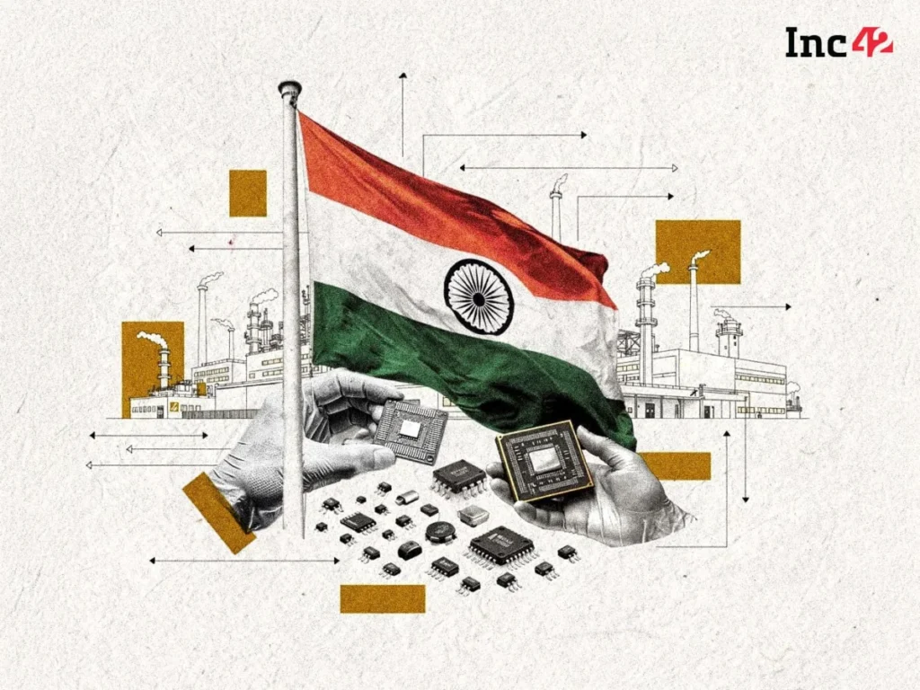
India’s quest to become a global powerhouse in the semiconductor value chain has hit a significant milestone. The Expenditure Finance Committee (EFC) of the Finance Ministry has officially cleared a ₹1.25 Lakh Crore proposal for the second phase of the India Semiconductor Mission (ISM 2.0). This pivotal development signals a strategic shift in New Delhi’s approach, moving from the initial "attraction phase" of semiconductor manufacturing to a more holistic, ecosystem-driven strategy.
With the EFC’s nod, the proposal is now headed to the Union Cabinet for final approval. Once greenlit, this massive financial outlay—nearly 65% higher than the ₹76,000 crore allocated to ISM 1.0—will serve as the bedrock for India’s next decade of technological sovereignty.
The Strategic Imperative: Why ISM 2.0 Matters
In an era defined by geopolitical volatility and the "chip war" between global superpowers, the fragility of the global technology supply chain has never been more apparent. India’s dependency on imported semiconductors for everything from smartphones and automobiles to defense systems remains a critical vulnerability.
ISM 2.0 is not merely an extension of the previous policy; it is a structural evolution. While the first phase focused on establishing the foundational pillars of fabrication (fabs) and assembly, testing, marking, and packaging (ATMP) units, the second phase aims to deepen the domestic footprint. The objective is clear: to insulate India from external supply shocks and position the nation as a trusted, resilient node in the global semiconductor architecture.
A Chronological Progression: From ISM 1.0 to 2.0
The journey of India’s semiconductor mission is a story of rapid policy maturation.
- December 2021: The Government of India launched the initial India Semiconductor Mission with an outlay of ₹76,000 crore, aiming to attract large-scale investments in fabs and display manufacturing.
- 2022–2023: The Ministry of Electronics and Information Technology (MeitY) rolled out the Design Linked Incentive (DLI) scheme, targeting the startup ecosystem and chip design firms to build local intellectual property (IP).
- March 2024: The Union Cabinet reached a landmark, approving the country’s first commercial semiconductor fab in Dholera, Gujarat, alongside other major ATMP facilities.
- July 2024: During the Union Budget for FY27, Finance Minister Nirmala Sitharaman formally announced the intent to launch ISM 2.0, emphasizing equipment, materials, and research.
- Late 2024: The Expenditure Finance Committee (EFC) clears the ₹1.25 Lakh Crore budget, paving the way for the next phase of the mission.
Supporting Data: The Current Ecosystem
The success of ISM 1.0 provides a strong baseline for the more ambitious second phase. To date, the government has approved 12 major semiconductor projects, securing cumulative investments of approximately ₹1.64 Lakh Crore.
Beyond fabrication, the design segment has shown remarkable resilience and growth. Under the DLI scheme, 24 semiconductor design projects have received government backing. Furthermore, the initiative has democratized access to technology, with over 100 companies utilizing advanced chip design tools. Data indicates that 23 chip tapeouts—a critical process of finalizing the design for manufacturing—have already been completed across various foundries. This serves as a testament to the growing prowess of Indian engineers in high-complexity chip architecture.
The Shift in Focus: What Defines ISM 2.0?
While the specific operational guidelines for ISM 2.0 are awaiting final Cabinet notification, the broad contours suggest a fundamental pivot. The "manufacturing-first" model is being expanded into a "full-stack" model.
1. Beyond Fabrication: Materials and Equipment
A significant portion of the new outlay is expected to support the manufacturing of semiconductor-grade chemicals, industrial gases, and sophisticated machinery. Currently, India imports the vast majority of these essential materials. By incentivizing local production, the government intends to lower the cost of manufacturing for fabs located within India, thereby increasing their global competitiveness.
2. recalibrating Incentives
Reports indicate that the government may rationalize the existing 50% capital expenditure subsidy for ATMP and OSAT facilities. The rationale is to move away from "blanket subsidies" toward performance-linked support that encourages value addition. By shifting focus to equipment and raw materials, the government hopes to create a self-sustaining cycle where the cost of building a chip is lowered through domestic availability of resources.
3. Strengthening the Design Pipeline
ISM 2.0 is expected to place a premium on indigenous IP. By linking incentives to capital raised from the market, the government aims to encourage startups to move from "service-based" design to "product-based" innovation. This "market-validated" approach ensures that only companies with real-world commercial viability receive state support.
Official Responses and Ministerial Vision
Electronics and IT Minister Ashwini Vaishnaw has repeatedly highlighted that the next phase of the mission is about "scale and depth." In various public forums, Vaishnaw has outlined a three-pronged vision for the next phase:
- Human Capital: Partnering with premier universities and research institutions to create a specialized workforce of engineers, material scientists, and process technicians.
- Supply Chain Integration: Ensuring that the global semiconductor supply chain views India as a strategic partner, not just a labor-intensive assembly hub.
- Indigenous IP: Moving toward "full-stack" Indian IP, which allows domestic companies to own the entire design-to-silicon lifecycle.
"The goal is to build an ecosystem where a chip designed in Bengaluru, manufactured in a fab in Gujarat, and packaged in a facility in Assam can compete with the best in the world," a senior official privy to the discussions noted.
Implications for the Industry
Industry leaders and stakeholders have largely welcomed the news, though they emphasize that the government’s role must extend beyond fiscal support.
The Need for "Patient Capital"
One of the most persistent demands from the startup ecosystem is the provision of "patient capital"—funding that can sustain the long gestation periods typical of semiconductor R&D. Industry experts argue that while the ₹1.25 Lakh Crore is a massive injection of funds, its success will depend on how easily companies can access this liquidity without being bogged down by bureaucratic hurdles.
EDA Tools and Software
The Electronic Design Automation (EDA) market is currently dominated by a few global giants. Stakeholders are pushing for the government to support domestic EDA tools, which would give Indian firms greater independence and reduce the royalties currently paid to foreign entities.
The Government as an "Anchor Customer"
Perhaps the most significant recommendation from industry analysts is for the state to become an early customer. By mandating the use of indigenous semiconductor technologies in government infrastructure, defense, and public utilities, the state can provide the initial demand volume necessary for startups to achieve economies of scale.
Conclusion: A Long-Term Strategic Bet
The ₹1.25 Lakh Crore allocation for ISM 2.0 is more than just a financial investment; it is a calculated bet on India’s future as a global technology hub. By addressing the gaps in materials, equipment, and research, the government is signaling that it is prepared to stay the course in a sector that requires immense patience and long-term commitment.
As India prepares to enter the next phase of its semiconductor journey, the focus will likely shift from the "quantity" of projects to the "quality" of integration. The road ahead is undoubtedly challenging, requiring tight coordination between the private sector, academia, and the state. However, with the structural foundations laid during ISM 1.0 and the broadened vision of ISM 2.0, India appears well-positioned to transform itself from a consumer of global silicon into a foundational contributor to the future of the digital world.