India Semiconductor Mission 2.0: Scaling the Silicon Frontier to Secure Global Dominance
NEW DELHI – In a move that signals a decisive shift from foundational capacity-building to deep-tech self-reliance, the Government of India has unveiled the “India Semiconductor Mission 2.0” (ISM 2.0) as a centerpiece of the Union Budget 2026-27. Building on the momentum generated by the initial iteration of the program, this second phase marks an ambitious evolution in the nation’s industrial strategy, moving beyond mere assembly and packaging to capture the high-value segments of the semiconductor value chain.
The announcement comes at a time when global geopolitical realignments are forcing nations to rethink their supply chain dependencies. By pivoting toward semiconductor equipment manufacturing, advanced materials, and the development of indigenous intellectual property (IP), India is positioning itself not just as a hub for chip assembly, but as a critical node in the global semiconductor ecosystem.
The Strategic Pivot: Decoding ISM 2.0
The primary objective of ISM 2.0 is to address the “missing links” in India’s domestic semiconductor ecosystem. While the first phase of the mission successfully attracted massive capital expenditure for fabrication (fabs) and Outsourced Semiconductor Assembly and Test (OSAT) facilities, the second phase is designed to nurture the “enablers” of the industry.
Core Focus Areas:
- Semiconductor Equipment Manufacturing: Encouraging domestic production of photolithography, etching, and deposition tools.
- Advanced Materials: Incentivizing the production of high-purity silicon, specialized gases, and chemicals required for wafer fabrication.
- Indigenous IP & R&D: Establishing design centers that focus on proprietary architecture, reducing reliance on foreign licensing.
- Supply Chain Resilience: Developing localized sourcing for raw materials to mitigate the impact of global trade volatility.
Chronology: A Trajectory of Growth
The journey to ISM 2.0 has been a calculated progression of policy and industrial diplomacy.
- December 2021: The Government of India announces the initial $10 billion (Rs 76,000 crore) incentive package for the semiconductor mission, aimed at attracting global manufacturing giants.
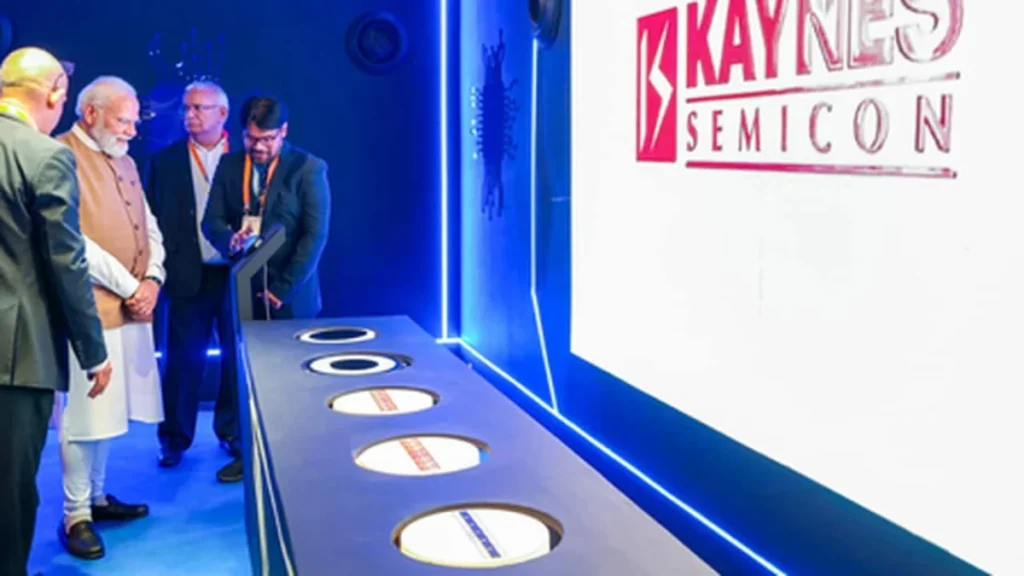
- 2023-2024: The first wave of “Mega Projects” gains traction. Major partnerships with global firms—including Micron, Tata Electronics, and Kaynes Technology—are formalized, setting the stage for domestic assembly and testing.
- 2025: The government completes a comprehensive audit of the initial program, identifying the need for a deeper localized supply chain. The focus shifts toward "Backward Integration."
- June 2026: Union Budget 2026-27 introduces ISM 2.0, explicitly detailing support for semiconductor equipment and raw material manufacturing. This announcement is accompanied by the approval of 12 new chip manufacturing projects, representing a massive Rs 1.64 lakh crore investment pipeline.
Supporting Data: The Scale of Investment
The numbers underpinning the current mission are staggering. With the approval of 12 new projects in June 2026, the cumulative investment pipeline in India’s semiconductor space has crossed the Rs 1.64 lakh crore mark.
| Segment | Investment (Approx. Rs Cr) | Strategic Focus |
|---|---|---|
| Foundry/Logic Fabs | 85,000 | Advanced node manufacturing |
| OSAT & Packaging | 45,000 | Testing and assembly efficiency |
| Materials/Equipment | 20,000 | Localizing the supply chain (New in ISM 2.0) |
| R&D and Design | 14,000 | Indigenous IP creation |
Beyond the capital outlay, the Ministry of Electronics and Information Technology (MeitY) estimates that these projects will generate over 250,000 high-skill jobs in the next five years, effectively creating a "silicon corridor" across states like Gujarat, Karnataka, and Tamil Nadu.
Official Responses: A Vision for “Atmanirbhar”
The government’s rhetoric surrounding ISM 2.0 is centered on the concept of Atmanirbhar Bharat (Self-reliant India).
"Semiconductors are the ‘oil’ of the 21st century," said a senior official from the Ministry of Finance during the post-budget briefing. "The first phase of the mission proved that India is an attractive destination for capital. The second phase is about proving that India can be an attractive destination for technology. We are no longer just looking for assembly lines; we are looking for the design, the equipment, and the materials that make the world run."
Industry leaders have largely welcomed the shift. A spokesperson for the India Electronics and Semiconductor Association (IESA) noted, "The focus on equipment and materials is the missing piece of the puzzle. By incentivizing the production of specialized gases and high-precision tools, the government is lowering the cost of entry for our local manufacturers and making our fabs more competitive globally."
Implications: A New Global Order
The launch of ISM 2.0 has profound implications for both the domestic economy and the global semiconductor landscape.
1. Strengthening the Global Supply Chain
By diversifying the manufacturing base away from traditional hubs like Taiwan and South Korea, India is providing a necessary “China+1” alternative. ISM 2.0 ensures that this alternative is not just a copy of existing models, but one that is vertically integrated.
2. The Rise of the Indian Design Ecosystem
With the focus on indigenous IP, India is transitioning from a service provider for global design firms to a creator of proprietary chip architectures. This will likely lead to a surge in semiconductor startups, fueled by the government’s commitment to R&D funding under the new mission.
3. Challenges and Hurdles
Despite the optimism, the path to success remains fraught with challenges. The semiconductor industry is notoriously capital-intensive and requires a steady, high-quality power supply and water infrastructure—areas where India continues to work on massive improvements. Furthermore, the global shortage of highly specialized talent—specifically in semiconductor physics and advanced lithography—remains a bottleneck that the government must address through academic partnerships and specialized vocational training.
Looking Ahead: The Decade of Silicon
As India moves into the second half of the decade, the success of ISM 2.0 will be measured by the "depth" of its ecosystem. The goal is to reach a stage where a semiconductor chip, from raw silicon wafer to final packaging, can be produced entirely within the country.
The Rs 1.64 lakh crore investment pipeline is not just a monetary figure; it is a testament to the long-term confidence global investors have in India’s regulatory environment. With the policy framework now extending to equipment and material localization, the barriers to entry for local players have been significantly lowered.
As we look toward the 2030 horizon, India’s semiconductor ambitions are no longer a distant dream. With the launch of ISM 2.0, the nation has laid the tracks for a high-speed technological revolution. The journey from being a consumer of technology to a foundational creator is well underway, and the next few years will prove whether India can successfully navigate the complexities of this ultra-competitive, high-stakes industry to emerge as a global leader in the silicon era.
Published: Jun 28, 2026 | Updated: Jun 28, 2026
Source: Industry Reports & Union Budget 2026-27 Official Documentation